Thrust B1 works on advancing 3D Laser Nanoprinting.
Thrust B1 focuses on bringing forward the technology and the machine tools for digital 3D Additive Manufacturing on the micrometer and nanometer scale by laser-based approaches, i.e., by 3D laser nanoprinting (sometimes also referred to as 3D direct laser writing). Previous work in this direction at KIT has led to the foundation of the company Nanoscribe GmbH (www.nanoscribe.de). In Thrust B1, we will tackle the three challenges “finer, faster, and more”.
1) At present, the minimum feature sizes are in the range of 100 nm. Stimulated-emission depletion (STED) inspired approaches have the potential for bringing us towards finer features in the 10 nm range.
2) Today, state-of-the-art laser-focus scanning speeds are in the range of 10 cm/s. Scalable approaches such as, e.g., using multiple laser foci have the potential to make 3D printing significantly faster.
3) The palette of accessible materials is limited. For example, electrically conducting or biodegradable 3D nanostructures are not readily available. Furthermore, 3D nanoprinting of many dissimilar ingredient materials within one 3D nanostructure is at its infancies. To this end, we will work towards wavelength-orthogonal printing and integrated microfluidics.
All of these scientific challenges have been described in much more detail in a comprehensive review article published in 2017 (https://onlinelibrary.wiley.com).
Thrust B1 will make advances in 3D laser nanoprinting immediately available to the users in Thrusts C1-C3 of this Cluster. Thrust B1 heavily relies on new photoresist systems, which we will investigate in close collaboration with Thrusts A3 and A2.
Thrust Spokespersons
Prof. Dr. Martin Wegener Karlsruhe Institute of Technology
Source: Hahn, V., Kiefer, P., Frenzel, T., Qu, J., Blasco, E., Barner-Kowollik, C., Wegener, M., Rapid Assembly of Small Materials Building Blocks (Voxels) into Large Functional 3D Metamaterials. Adv. Funct. Mater. 2020, 1907795. 10.1002/adfm.201907795.
You are currently viewing a placeholder content from Youtube. To access the actual content, click the button below. Please note that doing so will share data with third-party providers.
Illustration of 3D laser nanoprinting (Source: 3DMM2O, Patrick Müller)
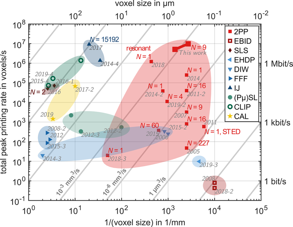
The 3D laser printing technology developed in the Cluster is put into perspective in the benchmark graphic. A continuously updated version of this benchmark graphic can be found on the website 3dprintingspeed.com.
Images
1.
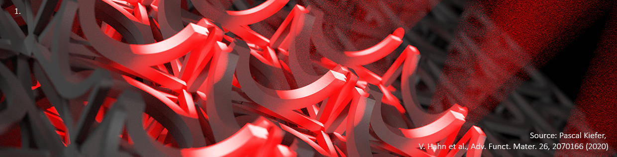
Description: Rapid multi‐focus multi‐photon 3D laser printing with an array of 3 × 3 laser foci that allows for sub‐micrometer voxel sizes at printing rates of about ten million voxels per second.(Source: Pascal Kiefer, V. Hahn et al., Adv. Funct. Mater. 26, 2070166 (2020))
2.
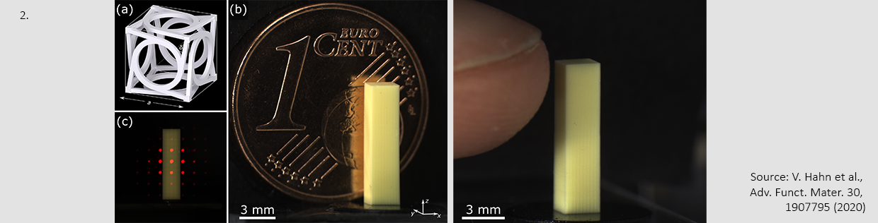
Description: Left side: a) Scheme of the chiral 3D metamaterial cubic unit cell with lattice constant a after ref. 48. b) Photograph of a manufactured chiral metamaterial sample (δ = 34.8°). This sample contains 30 × 30 × 120 = 108 000 3D unit cells with a = 80 µm (which is identical to the focus spacing in the laser‐focus array), thus a volume of 2.4 × 2.4 × 9.6 mm3. The sample contains about 3 × 10¹¹ voxels printed with a peak printing rate of 0.9 × 10⁷ voxels s−1. c) Laue diffraction pattern of the cubic metamaterial crystal upon exposure with laser light of 633 nm wavelength. This photograph has intentionally been overexposed to reveal the higher diffracted orders. A photograph of the sample has been added for clarity. Right side: Scale of the chiral metamaterial in comparison to a human thumb. (Source: V. Hahn et al., Adv. Funct. Mater. 30, 1907795 (2020))
3.
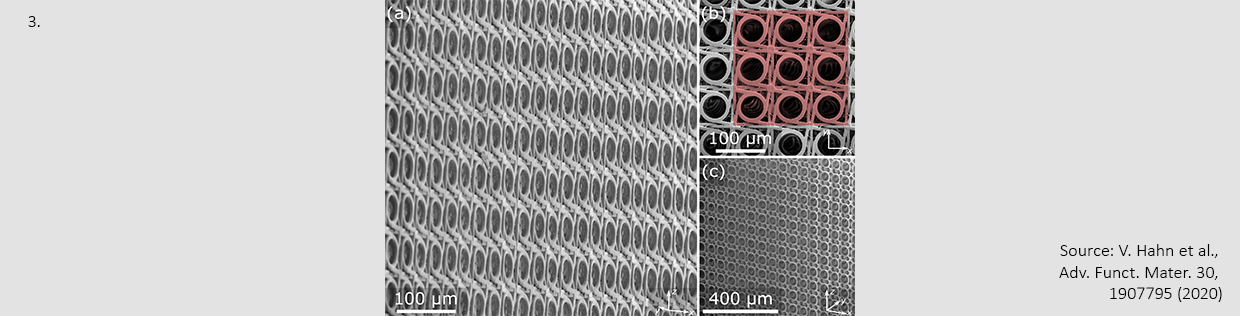
Description: a) Oblique side‐view scanning electron micrograph (cf. Figure 4b) of a 3D printed chiral mechanical metamaterial as in Figure 4 with δ = 34.8°. b) Top view exhibiting minor stitching artifacts caused by either the different foci in the 3 × 3 array and/or the adjacent writing fields. The simultaneously printed 3 × 3 array is highlighted in red. c) Achiral version of the metamaterial with δ = 0°. (Source: V. Hahn et al., Adv. Funct. Mater. 30, 1907795 (2020))